

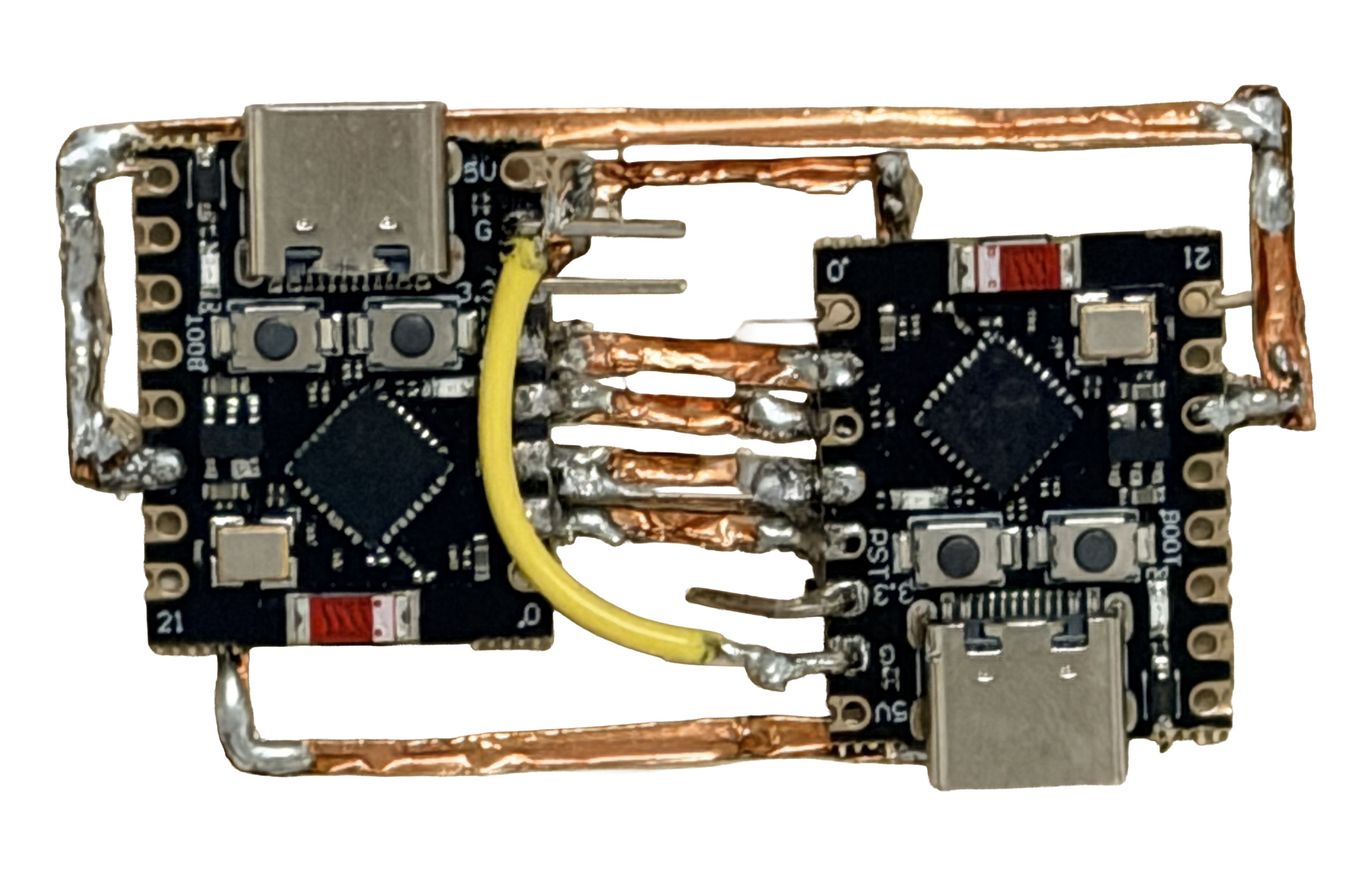
I've been sharing my build journey over on r/esp32, and one post hit a nerve I did not see coming: a photo of a genuinely ugly little board, two ESP32-C3s and a sensor wired up with copper tape on a 3D printed base. It picked up a few hundred upvotes and a comment section full of good questions. So I want to give it the writeup it earned: why I went the fast, ugly, 3D-printed-PCB route in the first place, how and when I knew it was time to stop taping copper down and lay out a real board, and what replaced it.
I did not expect that many of you to show up. Some asked "is that copper tape?" (yes). A few gently pointed out that my solder blobs were, and I quote, all peaky and not really blobs at all (also correct, I have since discovered flux, thank you). And a good handful asked the same thing: can you drop the STL?
So this post is all of that. The good, the ugly, the juicy stuff (the STL), and the honest part about when a hack has done its job and it's time to build the real thing.
Why build a PCB out of tape
I needed a custom board for a two-radio project (more on the two radios in a second), and I did not want to wait a week for a fab run just to find out I got a pin wrong. I also did not want a rat's nest of jumper wires that falls apart the moment you breathe on it. My first beta was exactly that, all wiring, and it was miserable to change.
Truth is, for the electrical side alone, you don't really need a custom PCB at all. A perfboard does the job, either soldered, or (as a few good folks reminded me in the thread) populated with pogo pins so you keep it light and can pull the boards back out. That part is solved cheaply.
For me the 3D printed board came from a different problem: packaging. Once the circuit worked, the questions became how do I wrap this up nicely, where do the traces actually travel, how does the geometry sit in a slick, small enclosure. I iterated over the shape several times, even stacked the boards at one point. And the two radios add a real constraint: point them the wrong way and they block each other, so they need a specific orientation. A perfboard does not decide that for you. A printed board does.
So the copper tape earns its place right there. You get real, flat, low-profile traces you can route however the enclosure wants, change them with a hobby knife in thirty seconds, and the whole thing lives in the 3D printed shell you were going to print anyway. It is not going to carry a lot of current or run at RF, but for wiring up dev boards, sensors, and power rails inside a shape you actually care about, it is genuinely great.
The how, the part you actually came for
Let me correct the record first, because a lot of people assumed the opposite: my board is soldered, and soldered well. The point was never to avoid solder. The point is that solder comes last, after the layout is right. You iterate the cheap, ugly way until the copper is exactly where it needs to be, and only then do you commit it. Get it right, then make it permanent.
The real method leans on a technique from this video, where he lays copper tape across the whole board and reveals the traces by abrasion instead of cutting them. Three moves:
1. A 3D printed baseplate with channels. You model shallow grooves where your traces need to run. Think of it as a breadboard you designed on purpose: the grooves are your routing.
2. Copper tape, pressed in deep. Lay adhesive copper foil over the whole board and press it hard into the grooves, all the way to the bottom, so the copper follows each channel and drops below the flat surface between them.
3. Sand it back smooth. Then sand the flat top face down. The copper sitting up on the flat comes off, the copper recessed down in the grooves survives, and you are left with clean, isolated traces sitting in their channels. Wipe it, then solder your connections onto them.
A real caveat on that last step: do not try the sanding pass on PLA. PLA is soft, and the sandpaper chews right through it and takes your traces with it. Use something that can actually take the abrasion, a tougher filament or a resin print, and it holds up fine.
That is the whole idea: the enclosure is the circuit. You print your routing, flood it with copper, sand it into a board, and solder it down.
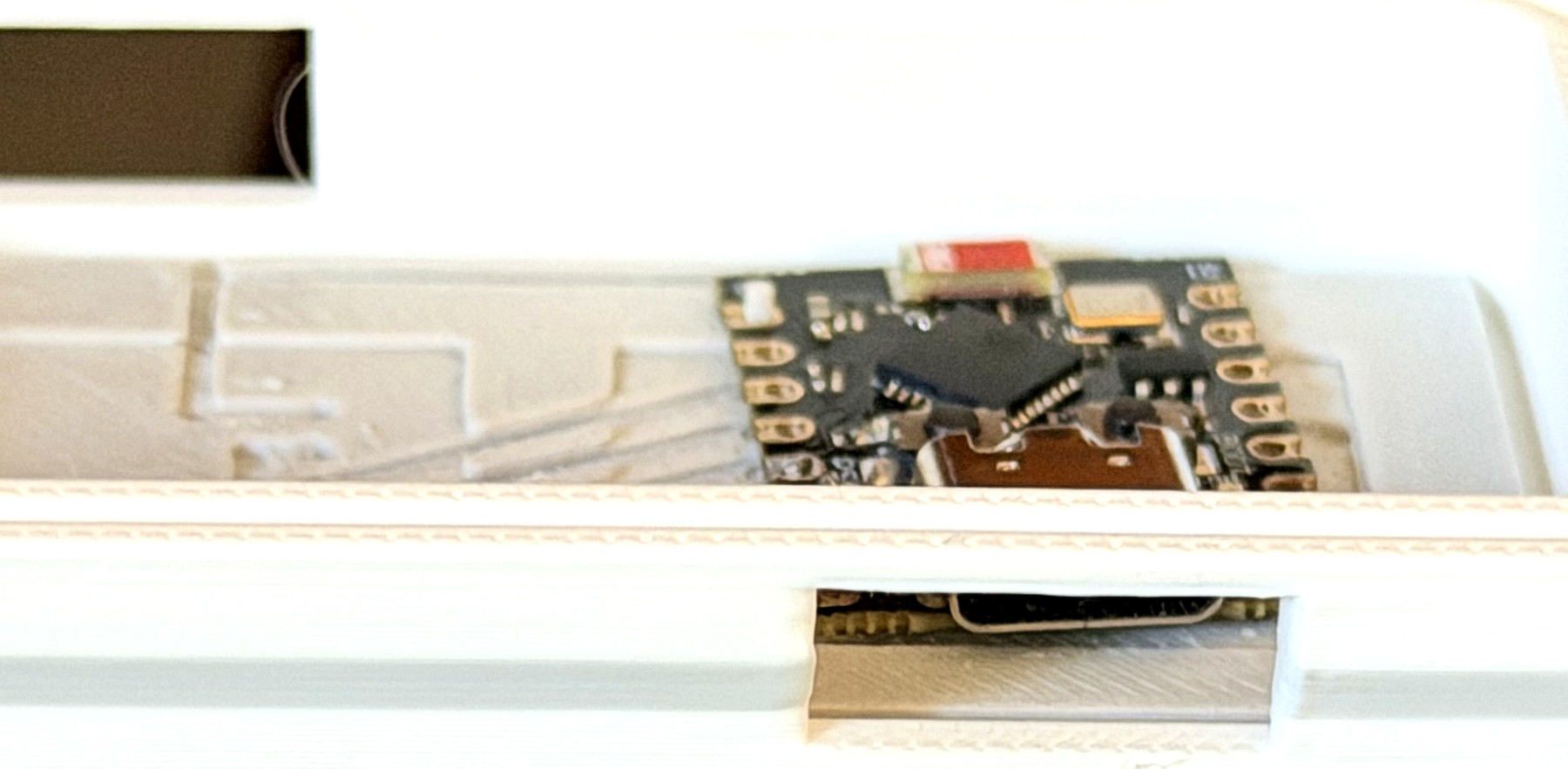
Now, a cleaner idea I did not use, but that came up in the thread and is genuinely good: skip the solder entirely and use pogo pins, little spring-loaded contacts seated in printed holes so they press against the tape when you clamp the lid on. That gets you a solder-free, pop-the-board-out-and-reuse-it version. I soldered mine because I wanted it permanent, but if you want reworkable, that is the move. Full credit to the folks who suggested it.
And one that took the whole thing further and I have not stopped thinking about: print the base in layers, each with grooves, stack them, and use little slices of metal tube as vias between layers. A DIY multilayer PCB with hidden routing. Have not tried it yet, but I will.
The STL, and the firmware to go with it
Straight up: I am not dropping the STL for my actual product board, the one with the specific SPI routing between the two chips. It is glued to one exact project and would just confuse you.
What I am giving you instead is better, because it is a real, buildable board, not a toy reference. It is the 3D-printed tape substrate for hms-mm, the fully open-source sibling of this project where the two ESP32-C3s talk over UART instead of SPI. Same technique you just read about, grooves and recessed pads and sanded-back copper, but simple enough that you can build it and have it actually do something.
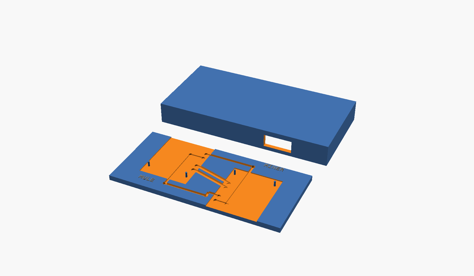
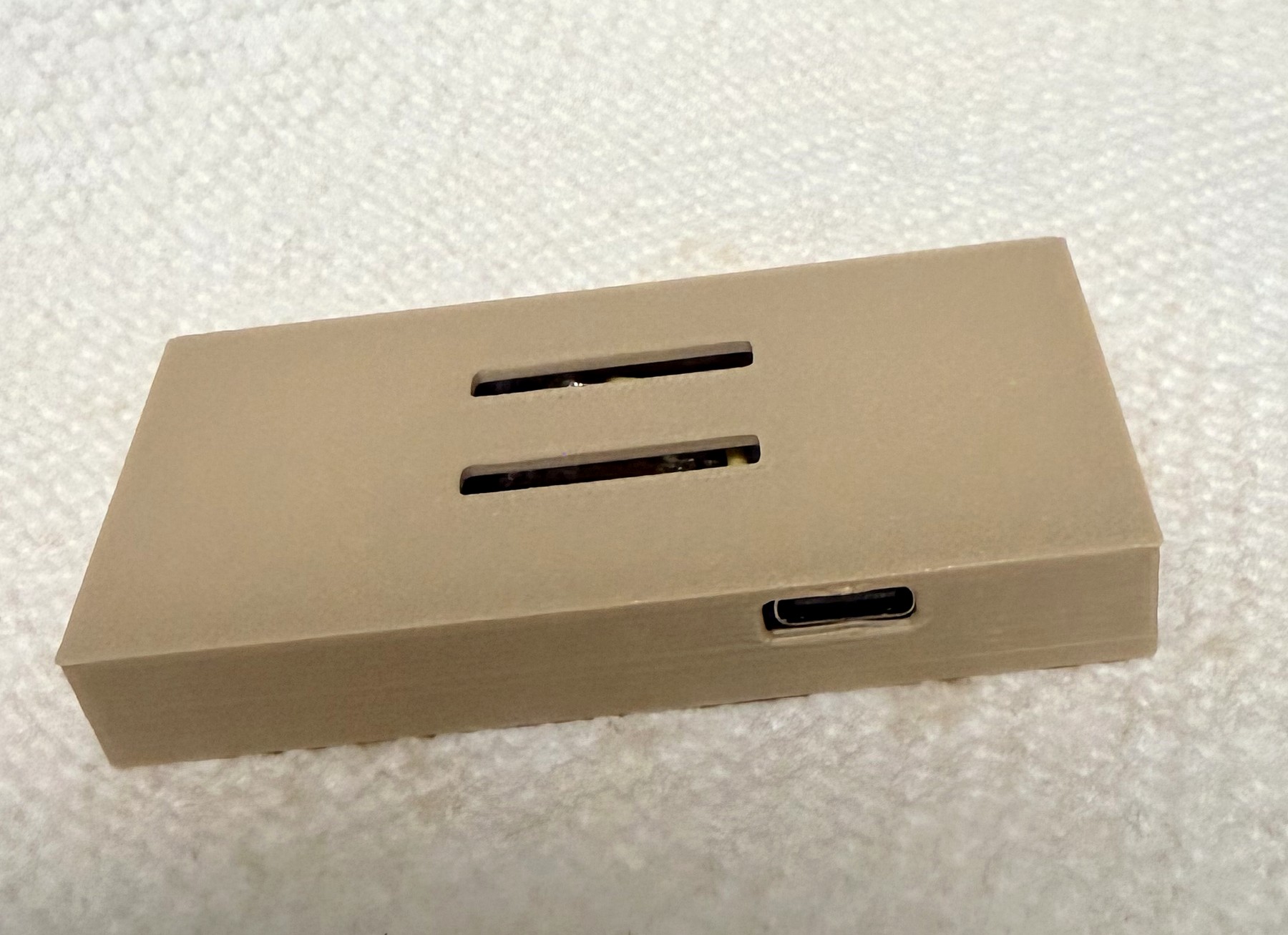
The routing is dead simple on purpose. The two UART lines cross the gap as parallel diagonals so there are no crossings to fight, and ground and a shared 3V3 rail loop back through the interior (so you can power the whole thing from either USB-C). Each SuperMini sits flush to its own edge, so its USB-C overhangs and a cable plugs straight in, and a slip-on lid (with a window for each port) closes the whole thing up. Print it in something tougher than PLA if you plan to sand the copper back, drop in two SuperMinis, then tape, sand, solder, flash, and cap it.
Download the STL. And as a bonus, the firmware for both the mule and the miner is open source too, right here: github.com/hms-homelab/hms-mm. Flash both boards, bridge them with tape, and watch one board pull data off a WiFi SD card while the other serves it back out on your own network. Go build it yourself. It is a genuine little treat the first time it comes alive:
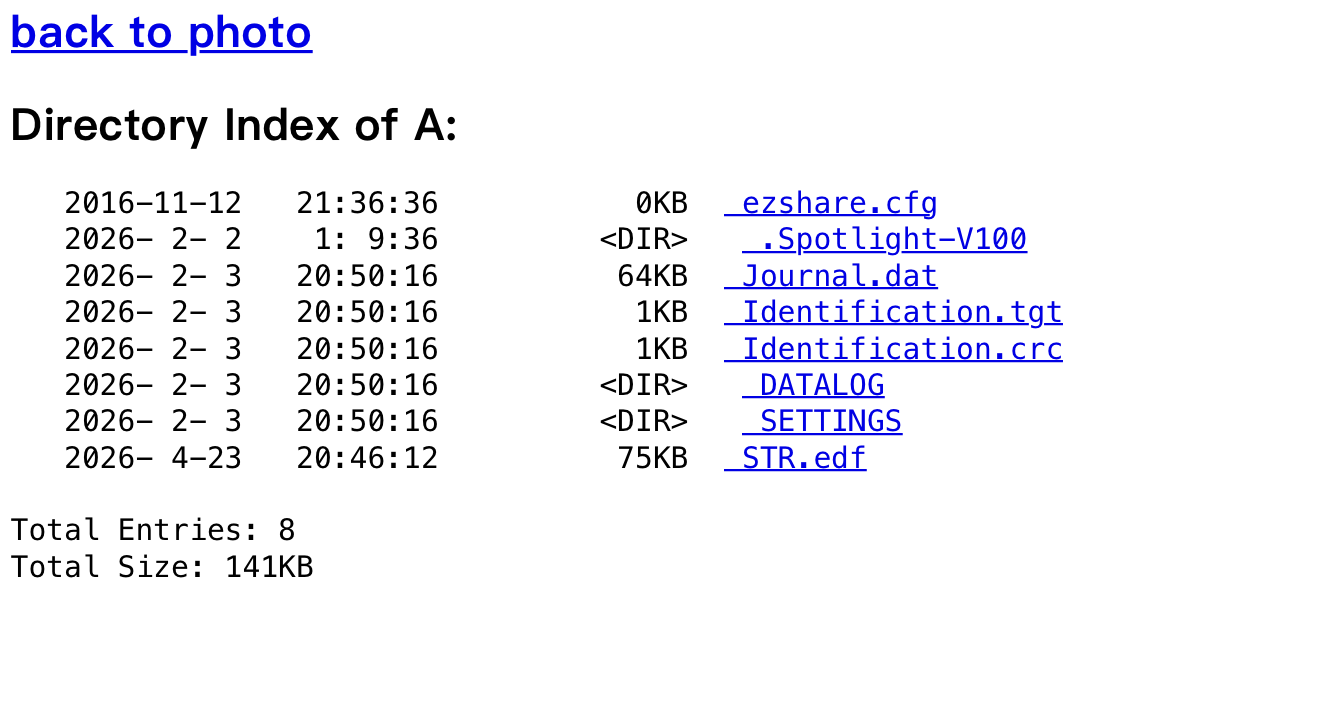
That is a real CPAP SD card, served straight off the little tape bridge over WiFi. From ugly copper foil to that.
If you want a ping when the next build goes up, the subscribe box near the top has you covered, but everything here is yours either way.
Knowing when the hack has done its job
The copper-tape board was never meant to last. It was a way to answer questions cheaply and fast. Is the pinout right? Do the two radios actually cooperate? Does the whole thing fit in the shell I want? Every one of those questions costs a week and a fab run to ask with a real PCB, or thirty seconds with a hobby knife on this one.
So I iterated on it, ugly and happy, until it stopped being the thing holding me back. And there is a moment where it flips. For me it was three signals at once:
- The layout stopped changing. I was not cutting new traces anymore, I was just re-taping the same one because it lifted.
- I needed more than one. A hack you build once is fine. The second time you rebuild it by hand, you are wasting your life.
- It had to be reliable, all night, unattended. Copper tape eventually lets go, and pogo pins are for the bench, not for something that has to run for years next to someone's bed while they sleep.
That last one was the tell. The prototype proved the idea worked. It could not be the idea. So I took everything it taught me, the pinout it had de-risked, the layout it had settled, and I drew a proper PCB. Real copper, real solder mask, plated through-holes, the works. That board is what the finished product runs on today. The ugly one got retired the day the real one came back from the fab and booted on the first try.
That is the whole point of a prototype like this. You are not building the product. You are buying certainty, cheaply, so that when you do spend the money on a real board, you already know it is going to work.
So what were the two ESP32s for?
This is the question that kept coming up in the thread, so here is the answer.
I needed two WiFi radios. One ESP32-C3 joins one network and quietly pulls data off a device on it, and the other joins a completely different network and serves that data out. One mines, one carries. A little two-headed bridge.
That sounds abstract until you know what it was bridging. The device on the first network is a CPAP machine, the breathing machine a lot of people use at night, and it writes a ton of detailed data to an SD card that almost nothing bothers to read. I wanted all of it, automatically, without ever pulling the card out. So the two boards became a tiny appliance that grabs that data off the machine's own WiFi and hands it to my phone and to the cloud, every morning, on its own.
I nicknamed the two boards the Mule and the Miner, and that ugly copper-tape prototype was their first working body. The clean version that came after it is a real product now.
If you want the engineering story of how the two boards actually talk to each other and pull it off, that is a rabbit hole worth falling into: start with So you bought the Mule and Miner, or the origin story in What is CpapDash, really. And if you just want to see what all that ugly copper tape was ultimately in service of, the dashboard is here.
Thanks for looking at my ugly board. Go make something worse, then make it work.